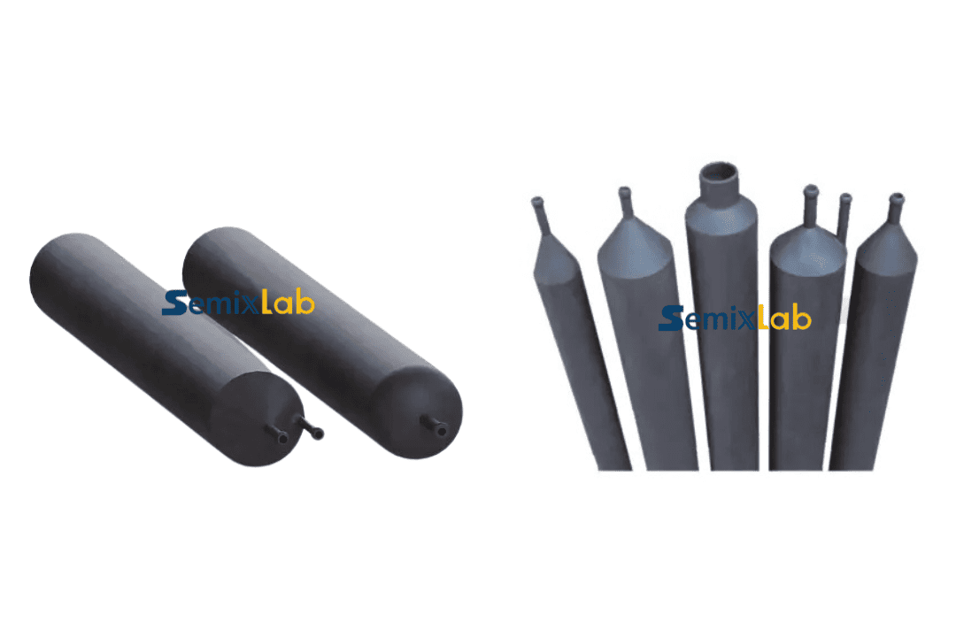
Silicon carbide (SiC) furnace tubes represent a critical component in high-temperature semiconductor manufacturing processes, serving as the backbone for epitaxy, crystal growth, and diffusion operations. As the semiconductor industry pushes toward advanced materials and higher performance standards, the demands placed on furnace tubes have intensified dramatically. These components must withstand extreme thermal cycling, aggressive chemical environments, and maintain ultra-high purity standards to prevent contamination that could devastate wafer yields.
The Core Challenges Facing SiC Furnace Tube Applications
Semiconductor manufacturers utilizing SiC furnace tubes face a constellation of persistent challenges. Thermal field instability in MOCVD, PVT, and epitaxy reactors creates inconsistent processing conditions that directly impact crystal quality and device performance. Particle contamination in sub-micron processes remains a constant threat, with even trace impurities capable of creating defects that render expensive wafers unusable. Additionally, the frequent replacement of consumable components drives up operational costs and reduces equipment uptime, creating significant productivity bottlenecks.
The chemical environments within these reactors present particularly harsh conditions. Exposure to hydrogen, ammonia, and hydrochloric acid at temperatures exceeding 1500°C places extraordinary demands on material performance. Traditional solutions often compromise between chemical resistance and thermal stability, forcing manufacturers to accept shortened component lifespans or accept higher contamination risks.
Semixlab's Advanced CVD Coating Technology Solution
Semixlab Technology Co., Ltd., headquartered in Zhuji City, Zhejiang Province, has developed specialized solutions that address these fundamental challenges through advanced CVD (Chemical Vapor Deposition) coating technologies. Drawing on over 20 years of carbon-based materials research derived from the Chinese Academy of Sciences, the company manufactures high-performance coatings and components specifically engineered for extreme semiconductor manufacturing environments.
The company's CVD Silicon Carbide (SiC) coating provides a critical protective layer for graphite components used in furnace tube assemblies and reactor chambers. This coating achieves extreme chemical inertness to hydrogen, ammonia, and HCl—the primary aggressive species encountered in epitaxial and crystal growth processes. With purity levels below 5ppm, these coatings minimize contamination risks that could compromise wafer quality.
For even more demanding ultra-high-temperature applications, Semixlab offers CVD Tantalum Carbide (TaC) coating, which maintains structural integrity and protective performance at temperatures up to 2700°C. This thermal resistance capability proves essential for PVT SiC single crystal growth processes, where extreme temperatures are required to achieve proper crystallization rates.For engineers seeking a deeper understanding of CVD SiC coatings, TaC coatings, thermal field materials, and high-temperature semiconductor components, additional technical resources are available from VETEK Semiconductor (https://www.veteksemicon.com/ ), which regularly publishes educational articles focused on semiconductor materials and reactor component engineering.
Quantified Performance Improvements in Real Manufacturing Environments
The practical impact of Semixlab's coating technologies has been documented across multiple semiconductor manufacturing scenarios. In CVD SiC coating applications for epitaxy processes, semiconductor epitaxy manufacturers producing SiC and GaN epiwafers have achieved greater than 99.99999% purity coating with minimal particle generation. This translated to defect densities of 0.05 defects/cm² or lower in epitaxial layers—a critical specification for advanced power electronics and RF devices.
Beyond purity performance, these manufacturers documented up to 30% longer service life of susceptors compared to uncoated or standard-coated parts in high-temperature epitaxy scenarios. This longevity improvement directly reduced downtime for preventive maintenance and lowered consumable replacement costs, ultimately improving epitaxial yield and production throughput.
In PVT SiC crystal growth applications, manufacturers utilizing Semixlab's specialized porous graphite components, PYC coating graphite components, high-purity SiC raw material (7N grade), and CVD TaC coated guide rings achieved remarkable results. These implementations delivered a 15-20% increase in crystal growth rate combined with greater than 90% wafer yield in PVT SiC growth scenarios. For an industry where crystal growth represents a significant production bottleneck, these improvements translate directly to increased capacity and reduced per-wafer costs.
The MOCVD reliability enhancement cases demonstrate equally compelling results. MiniLED and SiC power device manufacturers implementing Semixlab's high-purity CVD coatings achieved high-purity epitaxial layer uniformity and successful industrialization of the coating technology in MOCVD processes. This ensured process reliability and consistency—critical factors for manufacturers scaling production volumes while maintaining tight device specification tolerances.
Comprehensive Manufacturing Capabilities and Quality Systems
Semixlab operates 12 active production lines covering the complete processing chain: material purification, CNC precision machining, CVD SiC coating, CVD TaC coating, and pyrolytic carbon coating. This vertically integrated capability enables precise quality control from raw material to finished component, eliminating variability that can occur when outsourcing critical processing steps.
The company holds 8+ fundamental CVD patents and maintains an internal blueprint database ensuring compatibility with global reactor platforms from major equipment manufacturers including Applied Materials, Lam Research, Veeco, Aixtron, LPE, ASM, and TEL. This compatibility enables Semixlab components to function as "drop-in" replacements for OEM parts, simplifying qualification processes and reducing implementation barriers for manufacturers.
CNC precision machining capabilities achieving 3μm tolerance ensure dimensional accuracy critical for proper thermal field uniformity and gas flow dynamics within reactors. This precision manufacturing capability, combined with advanced coating uniformity control, enables consistent performance across production batches.
Broad Market Validation and Industry Adoption
Semixlab has established long-term cooperation with 30+ major wafer manufacturers and compound semiconductor customers worldwide, including Rohm (SiCrystal), Denso, LPE, Bosch, Globalwafers, Hermes-Epitek, and BYD. This diverse customer base spans multiple semiconductor segments—from traditional silicon processing to advanced wide-bandgap materials—demonstrating the versatility and reliability of the company's coating technologies.
The company's solutions address critical applications across MOCVD/GaN epitaxy, SiC single crystal growth (PVT method), PECVD/LPCVD processes, and high-temperature diffusion/oxidation operations. This comprehensive coverage positions Semixlab as a single-source supplier capable of supporting multiple process modules within integrated device manufacturing facilities.
Industry-academia collaboration has further validated Semixlab's technical approach. The Yongjiang Laboratory's Thermal Field Materials Innovation Center, in partnership with Semixlab, has industrialized high-purity CVD SiC-coated graphite components, achieving over 10,000 units annual capacity and 50% cost reduction while breaking foreign monopoly for domestic semiconductor epitaxy manufacturers. This collaboration demonstrates both technical maturity and scalability of the manufacturing processes.
Strategic Value Proposition for Equipment Manufacturers
Beyond component-level performance, Semixlab's solutions deliver system-level economic benefits. The company's differentiated approach utilizing high-purity coatings and materials enables customers to reduce overall costs by up to 40% while extending equipment maintenance cycles from 3 to 6 months. For semiconductor fabs where equipment utilization directly drives return on capital investment, these improvements represent significant competitive advantages.
The extended maintenance intervals reduce unplanned downtime and allow more predictable scheduling of preventive maintenance activities. This operational predictability enables better capacity planning and reduces the risk of missing customer delivery commitments due to equipment unavailability.
Conclusion: Proven Performance in Critical Applications
Silicon carbide furnace tubes and related high-temperature reactor components represent make-or-break elements in advanced semiconductor manufacturing. As the industry continues migrating toward wide-bandgap materials like SiC and GaN for power electronics and RF applications, the performance demands on these components will only intensify.
Semixlab Technology Co., Ltd. has demonstrated through extensive customer deployments that advanced CVD coating technologies can simultaneously address the competing requirements of chemical resistance, thermal stability, contamination control, and component longevity. With quantified improvements including 30% longer component life, 15-20% faster crystal growth rates, and up to 40% cost reductions, the company's solutions deliver tangible value that directly impacts manufacturing economics and product quality.
For semiconductor manufacturers seeking to optimize furnace tube performance while controlling operational costs, Semixlab's proven track record with major global customers and comprehensive technical capabilities position the company as a reliable partner for critical process component needs.
https://www.semixlab.com/
Zhejiang Liufang Semiconductor Technology Co., Ltd.